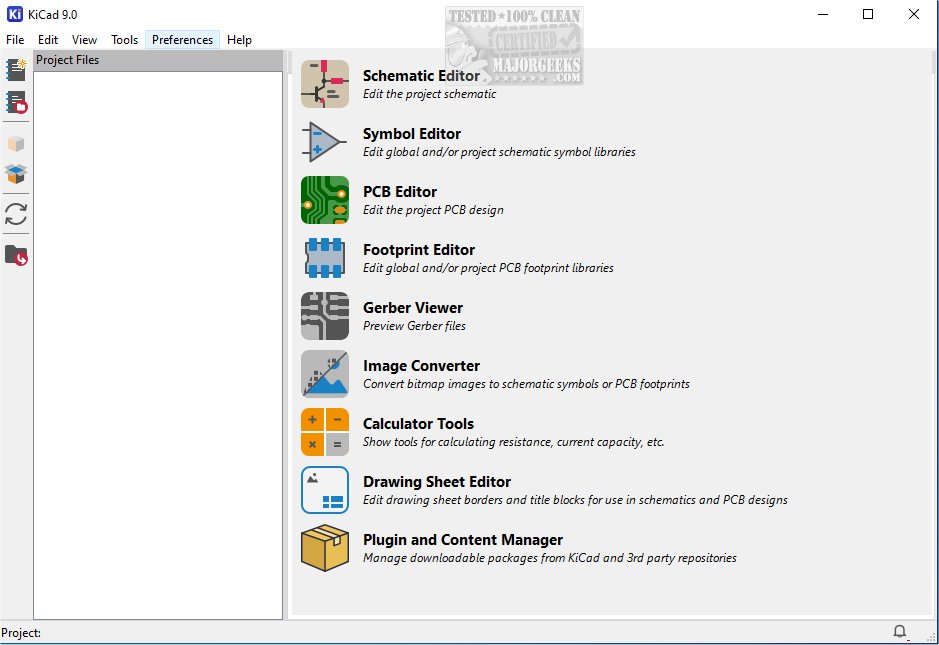
KiCad 9.0.8 has been released, enhancing its reputation as a leading cross-platform, open-source suite designed for electronics design automation. This software excels at managing both schematic capture and printed circuit board (PCB) layout, making it an invaluable tool for engineers and hobbyists alike. Notably, KiCad supports various output formats, including Gerber files and IPC-2581, which are essential for a wide range of design applications.
KiCad's integrated workflow facilitates the creation of schematic diagrams and PCB layouts in a cohesive manner, ensuring consistency and reducing errors throughout the design process. Users can design and modify electrical schematics that visually represent the connections and components of electronic circuits, which are vital for understanding functionality and planning layouts for projects.
The software provides an extensive array of tools for PCB layout, allowing for easy placement of components such as resistors, capacitors, and integrated circuits. Advanced routing capabilities enable the connection of these components with traces, effectively mirroring the pathways found in physical circuits. Design parameters like trace width and clearance can be meticulously adjusted to optimize electrical performance and manufacturability.
Once designs are finalized, KiCad generates essential manufacturing files, including Gerber files and Bill of Materials (BOM), streamlining the production process. Its intuitive interface and comprehensive features make it a go-to resource for both seasoned professionals and enthusiastic hobbyists in electronics.
In addition to its core functionalities, KiCad includes several utilities that enhance the design experience. A PCB calculator assists with important calculations related to trace width, current capacity, and voltage drop, while a built-in Gerber viewer allows users to inspect manufacturing files to ensure they meet fabrication standards. Furthermore, an integrated SPICE simulator enables detailed circuit analysis, allowing engineers to validate and simulate designs under various conditions before physical prototyping.
Overall, KiCad is recognized for its powerful capabilities and user-friendly design, making it a favored choice among PCB designers and electronic circuit developers. For users seeking greater flexibility, a portable version is available through MajorGeeks. New users are encouraged to explore the documentation provided to maximize their experience with this robust tool.
As electronic design continues to evolve, KiCad is expected to introduce further enhancements and features, solidifying its position as a vital resource in the field of electronics design. The community-driven development model promises ongoing improvements and support, ensuring that users can rely on KiCad for their future design projects
KiCad 9.0.8 released
KiCad: A cross-platform, Open Source suite for electronics design automation that effectively manages schematic capture and PCB (printed circuit board) layout. MajorGeeks also has the portable version.